Fraud Blocker Skip to main content

Materials Science Collection

"Exploring the Fascinating World of Materials Science

Background imageMaterials Science Collection: Woven fabric, SEM

Woven fabric, SEM
Woven fabric fibres. Coloured scanning electron micrograph (SEM) of synthetic fibres woven to form clothes. Nylon and polyester are common synthetic clothing materials

Background imageMaterials Science Collection: Nanotube technology

Nanotube technology. Computer artwork of four cylindrical fullerenes (carbon nanotubes) of varying size, with the smaller ones nested inside the larger ones

Background imageMaterials Science Collection: Nylon comb advert from DuPont, 1952 C019 / 1284

Nylon comb advert from DuPont, 1952 C019 / 1284
Nylon comb advert from DuPont. Advert for DuPont nylon combs and toothbrushes, from the August-September 1952 issue of the DuPont Magazine (volume 46, number 4, page 44)

Background imageMaterials Science Collection: SEM of a hooks and loops fastener

SEM of a hooks and loops fastener
Coloured scanning electron micrograph (SEM)of a hooks and loops fastener. It is a two-sheet material that is used as a reversible fastener on clothing and fabrics

Background imageMaterials Science Collection: Nanotube technology, conceptual artwork

Nanotube technology, conceptual artwork
Nanotube technology. Conceptual computer artwork of a woman wearing a hat that represents carbon nanotube technology. The hat is in the form of a molecular model that shows the hexagonal carbon

Background imageMaterials Science Collection: Buckyball molecule

Buckyball molecule. Computer artwork of a molecule of buckminsterfullerene (C60), a spherical fullerene and the first fullerene to be discovered (in 1985)

Background imageMaterials Science Collection: Czochralski silicon crystal growth

Czochralski silicon crystal growth
Silicon crystal growth. Artwork showing the industrial Czochralski process used to grow silicon crystals. Polycrystalline silicon (top left)

Background imageMaterials Science Collection: Raman laser spectroscopy C016 / 3827

Raman laser spectroscopy C016 / 3827
Raman laser spectroscopy. Researcher observing laser beams and microscope objectives. This LabRAM HR Raman laser spectrometer is being used to obtain phase

Background imageMaterials Science Collection: X-ray crystallography C016 / 3824

X-ray crystallography C016 / 3824
X-ray crystallography. Researcher using an X-ray machine to obtain crystal diffraction patterns of proteins for 3-D imaging of enzymes

Background imageMaterials Science Collection: FE scanning electron microscopy C016 / 3821

FE scanning electron microscopy C016 / 3821
FE scanning electron microscopy. Researcher operating a field-emission scanning electron microscope (FE-SEM). This is a F JEOL 6320F FE-SEM

Background imageMaterials Science Collection: Scanning transmission electron microscopy C016 / 3815

Scanning transmission electron microscopy C016 / 3815
Scanning transmission electron microscopy. Researcher using a scanning transmission electron microscope (STEM) to analyse the structure of solid-state materials

Background imageMaterials Science Collection: Metal-cutting tool production

Metal-cutting tool production. Close-up of a plate of cubic boron nitride being cut with a laser at the Microbor Nanotech factory, Moscow, Russia

Background imageMaterials Science Collection: Solar cell F008 / 4434

Solar cell F008 / 4434
Solar cell. Close-up of a high performance solar cell made from a monocrystalline silicon wafer. The contact grid is made from busbars (large strip) and fingers (small strips)

Background imageMaterials Science Collection: Solar cell F008 / 4431

Solar cell F008 / 4431
Solar cell, computer enhanced image. High performance solar cell made from a monocrystalline silicon wafer. The contact grid is made from busbars (larger vertical strips)

Background imageMaterials Science Collection: Solar cell F008 / 4428

Solar cell F008 / 4428
Solar cell. Close-up of a high performance solar cell made from a monocrystalline silicon wafer. The contact grid is made from busbars (large strip) and fingers (small strips)

Background imageMaterials Science Collection: Solar cell F008 / 4437

Solar cell F008 / 4437
Solar cell, computer enhanced image. Close-up of a high performance solar cell made from a monocrystalline silicon wafer. The contact grid is made from busbars (larger vertical strips)

Background imageMaterials Science Collection: Solar cell F008 / 4438

Solar cell F008 / 4438
Solar cell. High performance solar cell made from a monocrystalline silicon wafer. The contact grid is made from busbars (larger vertical strips) and fingers (small horizontal strips)

Background imageMaterials Science Collection: Solar cell F008 / 4433

Solar cell F008 / 4433
Solar cell. Close-up of a high performance solar cell made from a monocrystalline silicon wafer. The contact grid is made from busbars (large strip) and fingers (small strips)

Background imageMaterials Science Collection: Synthetic cork, SEM

Synthetic cork, SEM
Synthetic cork. Coloured scanning electron micrograph (SEM) of a section through a plastic wine bottle cork. The air holes within the cork allow it to shrink and expand to fit the bottle neck

Background imageMaterials Science Collection: Solar cell F008 / 4439

Solar cell F008 / 4439
Solar cell. Computer enhanced close-up of a high performance solar cell made from a monocrystalline silicon wafer. The contact grid is made from busbars (large strip) and fingers (small strips)

Background imageMaterials Science Collection: Faraday on metals and magnetism, 1847

Faraday on metals and magnetism, 1847
Faraday on metals and magnetism. Page from the notebooks of British physicist Michael Faraday (1791-1867), showing notes and a table of magnetic properties of a range of metals

Background imageMaterials Science Collection: Exoskeleton clothing, artwork C016 / 7702

Exoskeleton clothing, artwork C016 / 7702
Exoskeleton clothing. Computer artwork of a man wearing a protective exoskeleton suit that fits under normal clothing

Background imageMaterials Science Collection: Spider silk research C016 / 9552

Spider silk research C016 / 9552
Spider silk research. Golden silk orb-weaver spider in a laboratory being used for research on spider silk proteins. A thin strand of silk is visible emerging from the spiders spinnerets (centre)

Background imageMaterials Science Collection: Adobe brickwork C016 / 9609

Adobe brickwork C016 / 9609
Adobe brickwork. Adobe is a building material that consists of sand, clay, water, and a fibrous or organic material. Examples of organic materials used include sticks, straw, and manure

Background imageMaterials Science Collection: Hip socket bone grafting, diagram C016 / 6786

Hip socket bone grafting, diagram C016 / 6786
Hip socket bone grafting. Diagram showing completed hip socket bone grafting as part of a total hip replacement operation

Background imageMaterials Science Collection: Hip socket bone grafting, diagram C016 / 6784

Hip socket bone grafting, diagram C016 / 6784
Hip socket bone grafting. Diagram showing the second stage in hip socket bone grafting as part of a total hip replacement operation

Background imageMaterials Science Collection: Hip socket bone grafting, diagram C016 / 6785

Hip socket bone grafting, diagram C016 / 6785
Hip socket bone grafting. Diagram showing the third stage in hip socket bone grafting as part of a total hip replacement operation

Background imageMaterials Science Collection: Hip socket bone grafting, diagram C016 / 6783

Hip socket bone grafting, diagram C016 / 6783
Hip socket bone grafting. Diagram showing the first stage in hip socket bone grafting as part of a total hip replacement operation

Background imageMaterials Science Collection: Solar cell C016 / 9016

Solar cell C016 / 9016
Solar cell. Close-up of the surface of a solar (photovoltaic) cell, which converts light into electrical energy. The cell is made from silicon (blue), a semi-conductor

Background imageMaterials Science Collection: Solar cell C016 / 9019

Solar cell C016 / 9019
Solar cell. Close-up of the surface of a solar (photovoltaic) cell, which converts light into electrical energy. The cell is made from silicon (blue), a semi-conductor

Background imageMaterials Science Collection: Controls of early electron microscope

Controls of early electron microscope
Electron microscope. View of a technician operating the controls of an early model of electron microscope. The cabinets either side of the frame are computers and control equipment

Background imageMaterials Science Collection: Vat colour dye research, 1940s C018 / 0657

Vat colour dye research, 1940s C018 / 0657
Vat colour dye research. Industrial chemist working on vat colour dyes in a laboratory at a factory. Vat colours are fast dyeing agents, and are used on cotton, viscose process rayon and linen

Background imageMaterials Science Collection: Rayon research, 1950s C018 / 0661

Rayon research, 1950s C018 / 0661
Rayon research. Close-up of an industrial chemist drawing out filaments of rayon from a test tube. Rayon is a polymer fabric that can be produced in a number of ways

Background imageMaterials Science Collection: Teflon research, 1940s C018 / 0646

Teflon research, 1940s C018 / 0646
Teflon research. Laboratory technician testing a piece of Teflon (polytetrafluoroethylene, PTFE), a DuPont industrial plastic

Background imageMaterials Science Collection: Lycra advert, 1966 C018 / 0603

Lycra advert, 1966 C018 / 0603
Lycra advert. 1966 advertisement for a bra with straps and panels elasticated with lycra. This advert was produced by the US company DuPont

Background imageMaterials Science Collection: Nylon toothbrush research, 1930s C018 / 0677

Nylon toothbrush research, 1930s C018 / 0677
Nylon toothbrush research. Laboratory assistant Edward Burke working on early designs of toothbrushes using nylon bristles. Nylon was a new material discovered by the DuPont Company in 1935

Background imageMaterials Science Collection: DuPont Deepwater factory site, 1935 C018 / 0624

DuPont Deepwater factory site, 1935 C018 / 0624
DuPont Deepwater factory site, aerial photograph. This view looks north-west over the Deepwater Point site, located in New Jersey, USA, on the eastern bank of the Delaware River

Background imageMaterials Science Collection: Hilaire de Chardonnet, French engineer C018 / 0622

Hilaire de Chardonnet, French engineer C018 / 0622
Hilaire de Chardonnet (1839-1924), French engineer. Chardonnet was a French engineer, chemist and industrialist who invented the process of manufacturing rayon

Background imageMaterials Science Collection: Discovery of nylon, 1941 re-enactment C018 / 0675

Discovery of nylon, 1941 re-enactment C018 / 0675
Discovery of nylon, 1941 re-enactment. DuPont chemist Julian Hill (1904-1996) carrying out a re-enactment in 1941 of the discovery of nylon in 1935

Background imageMaterials Science Collection: Teflon research, 1940s C018 / 0647

Teflon research, 1940s C018 / 0647
Teflon research. Laboratory technician carrying out a test to compare Teflon with another plastic. She has dipped rods of the two plastics in a boiling bath of hot sulphuric acid

Background imageMaterials Science Collection: Rayon research, 1950s C018 / 0655

Rayon research, 1950s C018 / 0655
Rayon research. Laboratory researcher testing viscosity in the viscose process used in the manufacture of rayon. Liquid viscose, under carefully controlled temperature

Background imageMaterials Science Collection: DuPont Experimental Station, 1950s C018 / 0626

DuPont Experimental Station, 1950s C018 / 0626
DuPont Experimental Station, aerial photograph. This research site for the DuPont company is located on the banks of the Brandywine Creek in Wilmington, Delaware, USA. It was established in 1903

Background imageMaterials Science Collection: Early nylon research, 1940s C018 / 0676

Early nylon research, 1940s C018 / 0676
Early nylon research. DuPont research chemist working with nylon 6-6, the original nylon polymer discovered in 1935. First synthesized in February 1935, this new polymer was later commercialised

Background imageMaterials Science Collection: Wallace Carothers, US chemist C018 / 0621

Wallace Carothers, US chemist C018 / 0621
Wallace Hume Carothers (1896-1937), US industrial chemist, handling a sample of neoprene. Carothers studied at the University of Illinois, receiving his doctorate in 1924

Background imageMaterials Science Collection: DuPont research, 1950s C018 / 0678

DuPont research, 1950s C018 / 0678
DuPont research. Industrial research chemist watching an organic reaction. The program of fundamental research in organic chemistry at DuPont began in 1927

Background imageMaterials Science Collection: DuPont Seaford factory site, 1940s C018 / 0627

DuPont Seaford factory site, 1940s C018 / 0627
DuPont Seaford factory site, aerial photograph. Located at Seaford, Delaware, USA, and established in 1939, this was the first nylon yarn factory of the DuPont Company

Background imageMaterials Science Collection: Solar cell C018 / 6405

Solar cell C018 / 6405
Solar (photovoltaic) cell, which converts light into electrical energy. The cell is made from silicon (blue), a semi-conductor

Background imageMaterials Science Collection: Solar cell C018 / 6396

Solar cell C018 / 6396
Solar (photovoltaic) cell, which converts light into electrical energy. The cell is made from silicon (blue), a semi-conductor


All Professionally Made to Order for Quick Shipping

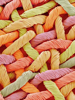
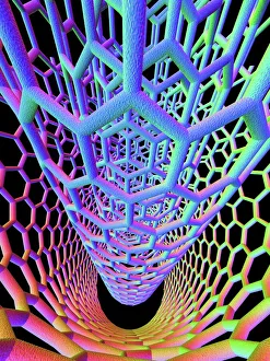
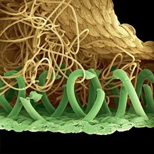
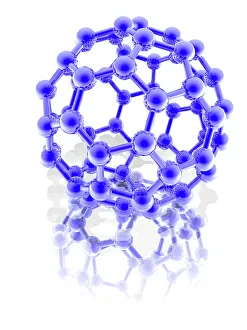
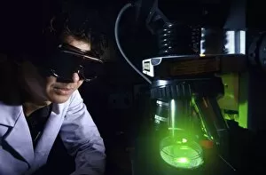
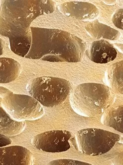
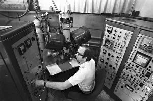
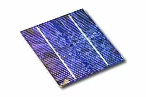
"Exploring the Fascinating World of Materials Science: From Woven Fabric to Nanotube Technology" a captivating field that delves into the intricate properties and applications of various substances. One such example is woven fabric, which showcases the artistry and functionality achieved through intertwining threads. With cutting-edge techniques like scanning electron microscopy (SEM), scientists can unravel the hidden structures within these fabrics, unlocking new possibilities for innovation. Nanotube technology takes materials science to another level by harnessing the power of tiny carbon cylinders. These nanotubes possess exceptional strength and conductivity, paving the way for advancements in electronics, medicine, and energy storage. Conceptual artwork visualizes their potential impact on our future. Looking back at history, we find intriguing artifacts like a 1952 DuPont advertisement featuring a nylon comb. This relic reminds us how materials have evolved over time, with DuPont's innovative approach shaping everyday objects we often take for granted. Microscopic images captured through SEM reveal astonishing details about hooks and loops fasteners—a testament to meticulous engineering behind Velcro-like closures that revolutionized industries from fashion to aerospace. The discovery of buckyball molecules opened up new frontiers in materials science. These soccer ball-shaped carbon structures exhibit extraordinary strength while offering exciting prospects in drug delivery systems or even as building blocks for advanced nanotechnology. Charcoal has long been used as an essential material due to its unique properties—absorption capabilities make it ideal for purifying air or water sources. Raman laser spectroscopy enables researchers to study charcoal's molecular composition further—uncovering its potential beyond traditional uses. X-ray crystallography provides invaluable insights into atomic arrangements within crystals—an indispensable tool in understanding material behavior ranging from minerals to pharmaceutical compounds. FE scanning electron microscopy allows scientists unparalleled resolution when investigating surface features at an atomic scale—an essential technique across diverse fields such as metallurgy or semiconductor research. Scanning transmission electron microscopy offers a deeper understanding of materials by mapping their elemental composition and electronic properties.