MEMS production

![]()
Wall Art and Photo Gifts from Science Photo Library
MEMS production
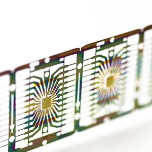
MODEL RELEASED. MEMS production. Clean room technician lifting a container of silicon wafers being used to produce MEMS (microelectromechanical systems) devices. The wafers will be placed in a furnace to deposit semiconductor films on their surfaces. MEMS devices are constructed on a microscopic scale using technologies such as wet and dry etching and thin film deposition. Applications include sensors and optical displays. Materials used to construct MEMS devices include silicon and polymers such as plastics. Photographed at an INEX facility. INEX is a British microsystems and nanotechnology company that was founded in 2002
Science Photo Library features Science and Medical images including photos and illustrations
Media ID 6436937
© COLIN CUTHBERT/SCIENCE PHOTO LIBRARY
2007 Assembling Clean Room Clean Room Suit Clothing Component Components Deposition Device Devices Electronics Engineer Factory Films Furnace Hi Tech Inex Manufacture Manufacturing Mechanical Mechanics Mems Mems Device Micro Microelectromechanical Systems Micromechanical Micromechanics Microsystems Nanotechnology New Castle Plates Producing Production Researcher Semi Conductor Sensor Sensors Silicon Silicon Plate Technician Thin Film Wafer Wafers Worker Laboratory
EDITORS COMMENTS
This print captures the intricate process of MEMS production, showcasing a clean room technician delicately lifting a container filled with silicon wafers. These wafers play a crucial role in manufacturing microelectromechanical systems (MEMS) devices, which are constructed on a microscopic scale using advanced technologies such as wet and dry etching and thin film deposition. The technician's precise movements highlight the meticulous nature of this industry, where even the tiniest components can have significant impacts. Once lifted from their container, these silicon wafers will undergo further processing in a furnace to deposit semiconductor films onto their surfaces. This step is essential for enhancing the functionality of MEMS devices. MEMS technology finds its applications in various fields including sensors and optical displays. The materials used for constructing these devices range from silicon to polymers like plastics, combining both mechanical and electronic elements seamlessly. Photographed at an INEX facility—a renowned British microsystems and nanotechnology company founded in 2002—this image showcases not only cutting-edge research but also the dedication of individuals working tirelessly behind closed doors. The clean room suit worn by the technician ensures that no contaminants interfere with this delicate process. Overall, this photograph serves as a testament to human ingenuity and technological advancements in the 21st century manufacturing industry. It encapsulates the fusion of science, engineering, and precision required to create innovative MEMS devices that shape our modern world.
MADE IN AUSTRALIA
Safe Shipping with 30 Day Money Back Guarantee
FREE PERSONALISATION*
We are proud to offer a range of customisation features including Personalised Captions, Color Filters and Picture Zoom Tools
SECURE PAYMENTS
We happily accept a wide range of payment options so you can pay for the things you need in the way that is most convenient for you
* Options may vary by product and licensing agreement. Zoomed Pictures can be adjusted in the Cart.