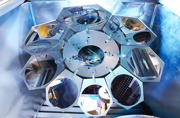
MEMS production, metal evaporation
![]()

Wall Art and Photo Gifts from Science Photo Library
MEMS production, metal evaporation
MEMS production. Inside of a metal evaporation machine that is being used to produce MEMS (microelectromechanical systems) devices. MEMS devices are constructed on a microscopic scale using technologies such as wet and dry etching and thin film deposition. This technique involves the use of an electron beam to evaporate metals and deposit them on a substrate, and is called e-beam metal evaporation. Applications of MEMS devices include sensors and optical displays. Materials used to construct MEMS devices include silicon and polymers such as plastics. Photographed at an INEX facility. INEX is a British microsystems and nanotechnology company that was founded in 2002
Science Photo Library features Science and Medical images including photos and illustrations
Media ID 6438137
© COLIN CUTHBERT/SCIENCE PHOTO LIBRARY
2007 Clean Room Component Components Device Devices Electronics Factory Hi Tech Inex Machine Manufacture Manufacturing Mechanical Mechanics Mems Mems Device Micro Microelectromechanical Systems Micromechanical Micromechanics Microsystems Nanotechnology Producing Production Semi Conductor Sensor Sensors Silicon Electron Beam Laboratory
EDITORS COMMENTS
This print showcases the intricate process of MEMS production, specifically metal evaporation. Inside a state-of-the-art metal evaporation machine at an INEX facility, cutting-edge technology is employed to create microelectromechanical systems (MEMS) devices on a microscopic scale. Utilizing advanced techniques like wet and dry etching and thin film deposition, this particular method involves the use of an electron beam to evaporate metals onto a substrate – hence its name, e-beam metal evaporation. The result is the construction of highly precise components that find applications in various fields such as sensors and optical displays. The materials used for these remarkable MEMS devices range from silicon to polymers like plastics. This fusion of materials allows for exceptional performance and durability in these tiny yet powerful creations. Science Photo Library's snapshot captures the essence of this industrial marvel, showcasing the convergence of research, technology, and manufacturing prowess in one frame. It symbolizes the relentless pursuit of progress in 21st-century industries where nanotechnology plays a significant role. While not explicitly mentioned by Science Photo Library due to commercial restrictions, it is fascinating to imagine how these MEMS devices could revolutionize our lives with their potential applications across electronics, mechanics, and sensors. This image serves as a testament to human ingenuity at work within clean rooms and laboratories worldwide as we continue pushing boundaries towards new frontiers in microtechnology.
MADE IN AUSTRALIA
Safe Shipping with 30 Day Money Back Guarantee
FREE PERSONALISATION*
We are proud to offer a range of customisation features including Personalised Captions, Color Filters and Picture Zoom Tools
SECURE PAYMENTS
We happily accept a wide range of payment options so you can pay for the things you need in the way that is most convenient for you
* Options may vary by product and licensing agreement. Zoomed Pictures can be adjusted in the Cart.

