Quality control of integrated circuit wafers
![]()

Wall Art and Photo Gifts from Science Photo Library
Quality control of integrated circuit wafers
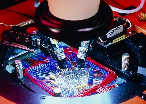
Quality control stage in the fabrication of silicon-based integrated circuit wafers, showing a close-up of a probe which automatically test the circuitry of each chip on the wafer. Any chips that are found to be faulty are marked with ink contained in the two pens visible in centre. After probing, a wafer is baked to harden the ink; defective chips may then be identified and discarded when the wafer is sawn into individual integrated circuits, ready for the attachment of connector wires and final packaging (encapsulation)
Science Photo Library features Science and Medical images including photos and illustrations
Media ID 6429363
© DAVID PARKER/SEAGATE MICROELECTRONICS LTD/ SCIENCE PHOTO LIBRARY
Chip Manufacture Electronic Electronics Integrated Circuit Micro Chip Probing Quality Control Semiconductor Industry Silicon Chips
EDITORS COMMENTS
This print from Science Photo Library showcases the meticulous process of quality control in the fabrication of silicon-based integrated circuit wafers. The image zooms in on a crucial stage, where a probe automatically tests the intricate circuitry of each chip on the wafer. With utmost precision, this advanced technology ensures that every chip meets stringent standards before progressing further. Intriguingly, any chips found to be faulty are marked with ink using two pens positioned at the center of the frame. This ingenious technique allows for easy identification and subsequent removal during later stages. To solidify these markings, the entire wafer is then baked to harden the ink effectively. The significance of this quality control stage becomes evident when we consider how these wafers are eventually transformed into individual integrated circuits. Once sawn into separate pieces, these circuits undergo final processing steps such as attaching connector wires and encapsulation for packaging. Within this mesmerizing snapshot lies an amalgamation of electronic marvels - microchips, semiconductor industry expertise, and cutting-edge electronics manufacturing techniques. It serves as a testament to human ingenuity and our relentless pursuit of perfection within technological advancements. Science Photo Library has once again captured an extraordinary moment in time that unveils both artistry and scientific rigor behind one of today's most critical industries – shaping our digital world through silicon chips.
MADE IN AUSTRALIA
Safe Shipping with 30 Day Money Back Guarantee
FREE PERSONALISATION*
We are proud to offer a range of customisation features including Personalised Captions, Color Filters and Picture Zoom Tools
SECURE PAYMENTS
We happily accept a wide range of payment options so you can pay for the things you need in the way that is most convenient for you
* Options may vary by product and licensing agreement. Zoomed Pictures can be adjusted in the Cart.

