
Materials Scientist Collection
Materials scientists are the unsung heroes of innovation, working tirelessly behind the scenes to unlock the secrets of various substances


All Professionally Made to Order for Quick Shipping
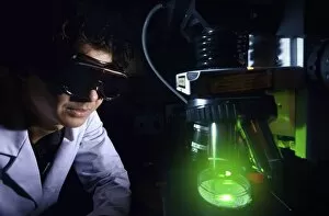
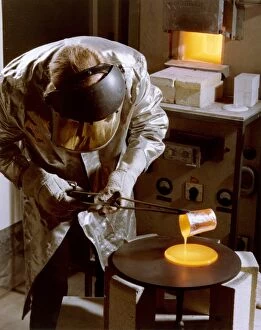
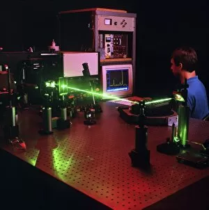
Materials scientists are the unsung heroes of innovation, working tirelessly behind the scenes to unlock the secrets of various substances. Armed with cutting-edge technologies like Raman laser spectroscopy, X-ray crystallography, and FE scanning electron microscopy, they delve into the microscopic world to understand materials at their core. With Raman laser spectroscopy (C016/3827), these scientists use light scattering techniques to analyze molecular vibrations and gain insights into a material's chemical composition. Meanwhile, X-ray crystallography (C016/3824) allows them to determine atomic arrangements within crystals with unparalleled precision. FE scanning electron microscopy (C016/3821) takes their investigations further by providing high-resolution images that reveal surface structures and topography in incredible detail. Similarly, scanning transmission electron microscopy (C016/3815) enables them to visualize even smaller features at an atomic level. In their pursuit of knowledge, materials scientists also employ micrography metallurgy analysis from 1937 (C014/0466). This historical technique helps them understand how metals behave under different conditions and refine manufacturing processes accordingly. Their quest for excellence extends beyond metals as they explore glass and ceramics research (C016/2053). By studying these versatile materials' properties and behavior, they contribute to advancements in fields ranging from architecture to electronics. The work of a materials scientist wouldn't be complete without tools like the silicon cluster manufacturing tool (C016/3822). This technology aids in creating intricate structures on silicon surfaces for applications such as semiconductors or nanotechnology devices. To unravel complex crystalline structures further, X-ray crystallography is employed once again but this time with C016 / 3823 code. The resulting data provides invaluable information about chemical bonding patterns within solids. Scanning electron microscopy continues its reign as one of their go-to methods through C016 / 3816 code.