
Metalloid Collection
"Unveiling the Enigmatic World of Metalloids: A Journey through Silicon and Boron" In the realm of materials science


All Professionally Made to Order for Quick Shipping
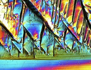
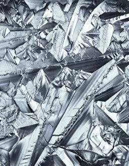
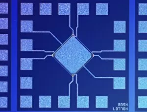
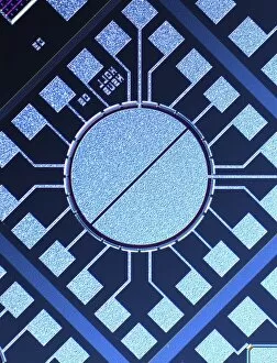
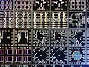
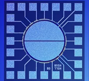
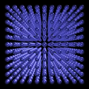
"Unveiling the Enigmatic World of Metalloids: A Journey through Silicon and Boron" In the realm of materials science, metalloids stand as fascinating entities that blur the line between metals and non-metals. Let's embark on a captivating exploration into their intricate nature. Firstly, we encounter a mesmerizing sight - a magnified view of a Silicon crystal. Its intricate lattice structure reveals its unique properties, making it an essential component in countless electronic devices that shape our modern world. Moving forward, we delve deeper into the atomic realm with an atomic model of Boron. This metalloid showcases exceptional strength while maintaining its ability to conduct electricity – qualities highly sought after in various industries. As we zoom out from the microscopic world, we are greeted by a breathtaking macrophotograph capturing another Silicon crystal. The sheer beauty lies within its delicate patterns and symmetrical arrangement—a testament to the elegance hidden within these enigmatic elements. Shifting gears towards technology's heart, we shift our focus onto microchips' surfaces. Through light micrographs, we witness their intricacy up close—each image revealing different facets of this technological marvel. The first glimpse shows us surface C018/6398—an awe-inspiring network resembling an interconnected cityscape where information flows ceaselessly like rivers through streets lined with transistors and circuits. Surface C018/6399 invites us further into this digital metropolis—the vibrant colors painting a picture of precision and complexity as electrons dance across meticulously etched pathways. Next comes surface C018/6390—a snapshot showcasing how every minuscule detail plays a crucial role in shaping our interconnected world. Each tiny feature contributes to seamless communication between devices that have become indispensable parts of our lives. Surface C018/6381 beckons us closer still—the interplay between light and shadow highlighting minute imperfections that engineers tirelessly strive to overcome for enhanced performance and efficiency.