
Nrel Collection
"NREL: Unveiling the Hidden World of Science and Technology" Step into the realm of cutting-edge research at NREL


All Professionally Made to Order for Quick Shipping
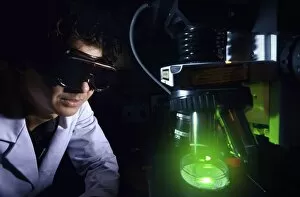
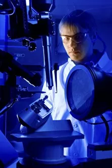
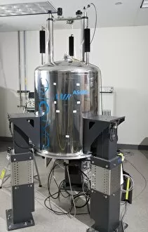
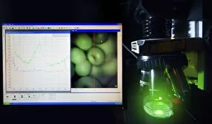
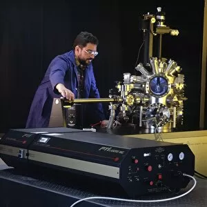
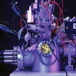
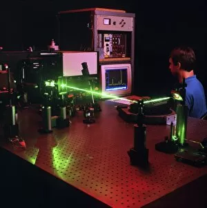
"NREL: Unveiling the Hidden World of Science and Technology" Step into the realm of cutting-edge research at NREL, where scientists utilize a myriad of advanced techniques to unravel the mysteries of our universe. With Raman laser spectroscopy (C016/3827), they delve deep into molecular structures, unlocking secrets that were once hidden from view. X-ray crystallography (C016/3824) allows them to peer into crystalline materials with unprecedented precision, revealing their intricate atomic arrangements. FE scanning electron microscopy (C016/3821) provides a glimpse into the microscopic world, capturing stunning images that showcase the beauty and complexity of nature's building blocks. Meanwhile, scanning transmission electron microscopy (C016/3815) takes us even further by enabling scientists to observe individual atoms in real-time, offering unparalleled insights into material properties. The Rutherford backscattering spectrometer (C016/3834) uncovers elemental composition with remarkable accuracy, shedding light on the fundamental building blocks of matter. The nuclear magnetic resonance spectrometer (C016/3830) delves deeper still by analyzing molecular interactions and dynamics within complex systems. NREL's pulse laser deposition apparatus (C016/3828) enables precise control over thin film growth processes for various applications ranging from electronics to energy storage. Photovoltaic cell testing (C016/3829) ensures efficient solar power conversion through rigorous evaluation and optimization. With additional tools like Raman laser spectroscopy (C016 / 3826), molecular beam mass spectrometry (CO16 / 3825), silicon cluster manufacturing tool (CO16 / 3822), and X-ray crystallography (CO16 / 3823), NREL continues to push boundaries in scientific exploration. At NREL, innovation knows no bounds as brilliant minds harness these state-of-the-art technologies to unlock new frontiers in science and technology.